Development of mass production testbench for IMX6 based hardware
Next step after PCB soldering in mass production of electronic hardware is testbench that performs initial firmware upgrade and basic testing of soldered devices. As well as PCB soldering operating with that testbench must be automated as much as possible. As a last resort, manual operations that could not be eliminated should be extremely simple, intuitive and monotonous.
Here described steps of developing such testbench (hardware and software both) for IMX6ULL based electronic device (SoM module). At the end of the article, the source code of the testbench (Python script) is provided, which can be adapted to other families of microprocessors based on ARM architecture.
So we made some SW development using development board and made sure that IMX6ULL suits us – necessary interfaces supported, CPU perfomance enough for our tasks and we got understanding of approximate size of final firmware. So now it is time to start hardware development (PCB design) based on that microprocessor.
Among other requirements to the PCB you need to consider following three questions:
- where to store Linux image to be used on CPU booting (SPI flash, NAND flash, microSD card or something else);
- how to burn that firmware to flash on mass production;
- how to set the booting interface of the processor;
Answer options for each question:
- The easiest way to use microSD card. In this case you only need to prepare some amount of microSD cards pre-flashed with kernel image and insert them to soldered devices. But this method may not work if:
- you need to design industrial grade device (operating temperatures starting from -40 C);
- you want to complicate access to firmware;
- the device may be subject to vibrations;
- you have strict limits on the BOM cost (a microSD card + connector is obviously more expensive than a flash memory chip soldered on the board);
- you have strict restrictions on the dimensions of the final product;
If the microSD card is not suitable, the choice remains between NOR and NAND memory. Here the most determining factor – is final firmware size. If lower that 32 Mb – better to use NOR as it cheaper and has more write cycles. If higher than 32 Mb – NAND.
2. If you chose flash IC then there are two options:
- the image is flashed into the IC before soldering it. In that case ICs need to be taken from reel one by one, burned using programmer (like this), then packed back to the reel. Very laborious and not technological option.
- the image is flashed into the IC after being soldered. Here we need help of microprocessor. CPU need to boot using any other booting option, receive firmware somehow and flash it to IC. Sound hard (or even impossible) in implementation but it reduces amount of manual operations in mass production. looking ahead, I’ll say that we chose this option and we managed to automate it
3. Using development boards, you’ve almost certainly seen something like this:
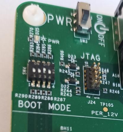
There is boot mode switch. Microprocessors, typically, supports use of different interfaces to access boot image such as SPI, QSPI, SDHC, UART, etc. Which boot option to use is determined by the fuse bits. The processor can take fuse bits from registers, either by determining the state of certain GPIOs. Which way the processor should use, in turn, is given by the state of the other two GPIO (BOOT_MODE0 and BOOT_MODE1).
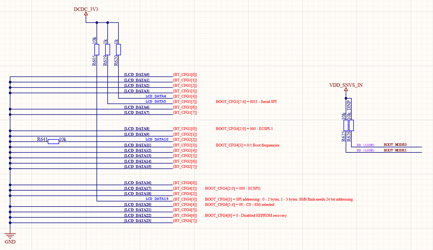
You can also find a variant of a single boot option specified by resistors:
In a case you are limited in PCB size (our case) or you need configuration gpios to be used in alternative way, then only the third option remains – to “burn” the fuse bit.
So, in our case, the answers to the three questions above were:
- The image is stored in a SPI NOR flash IC;
- The memory IC is flashed already being soldered on the board;
- “Burning” fuse beats
Testbench itself
The solution of the problem in this formulation of the questions was the developed testbench of serial flashing and initial testing.
The device for which the testbench was designed:
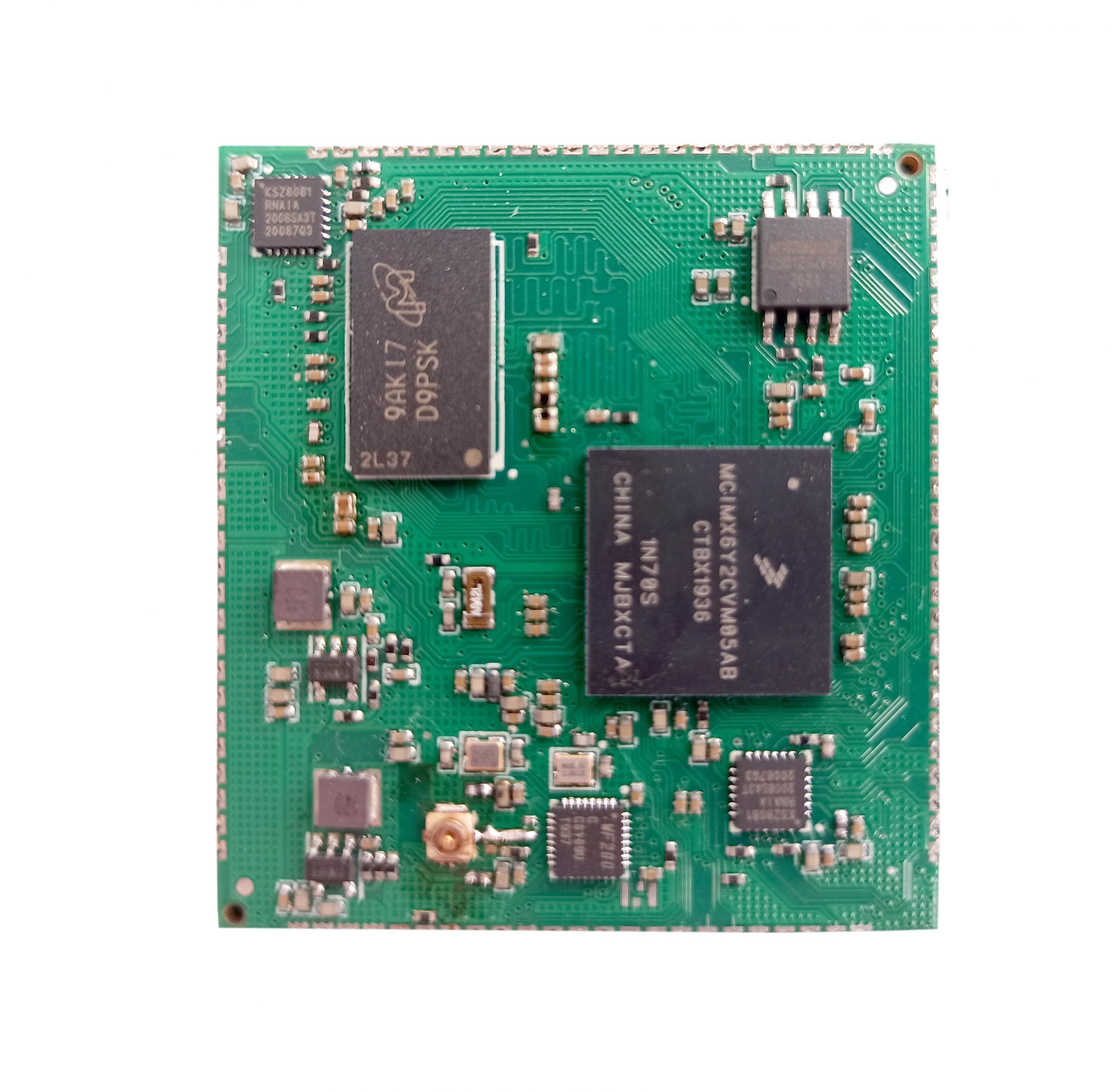
SoM module with typical set of ICs: CPU, DDR3 IC, SPI flash IC, Ethernet PHY IC, Wi-Fi PHY IC. On all four surfaces there are half-via pads with a 1.5mm pitch.
Here is testbench itself:
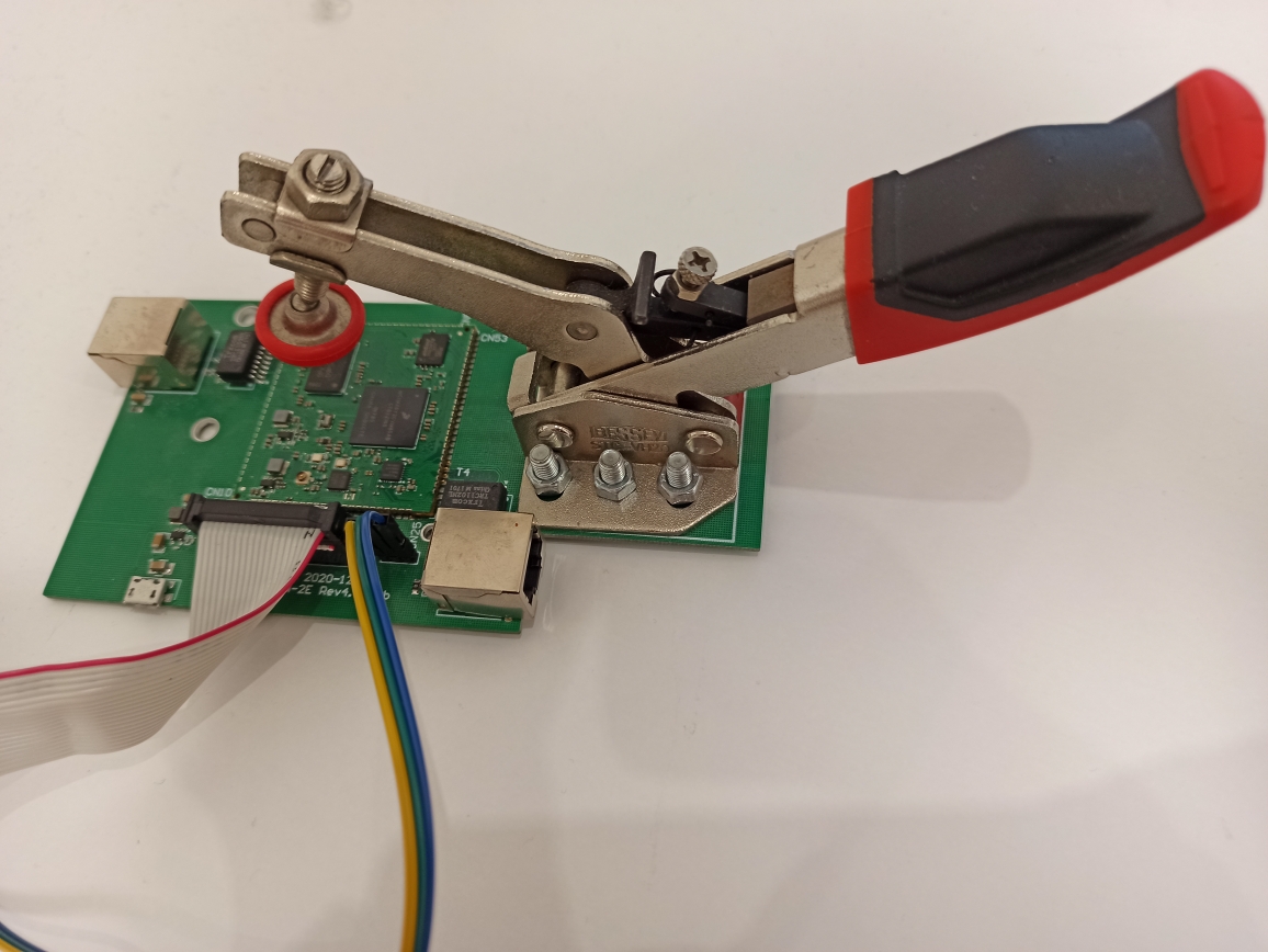
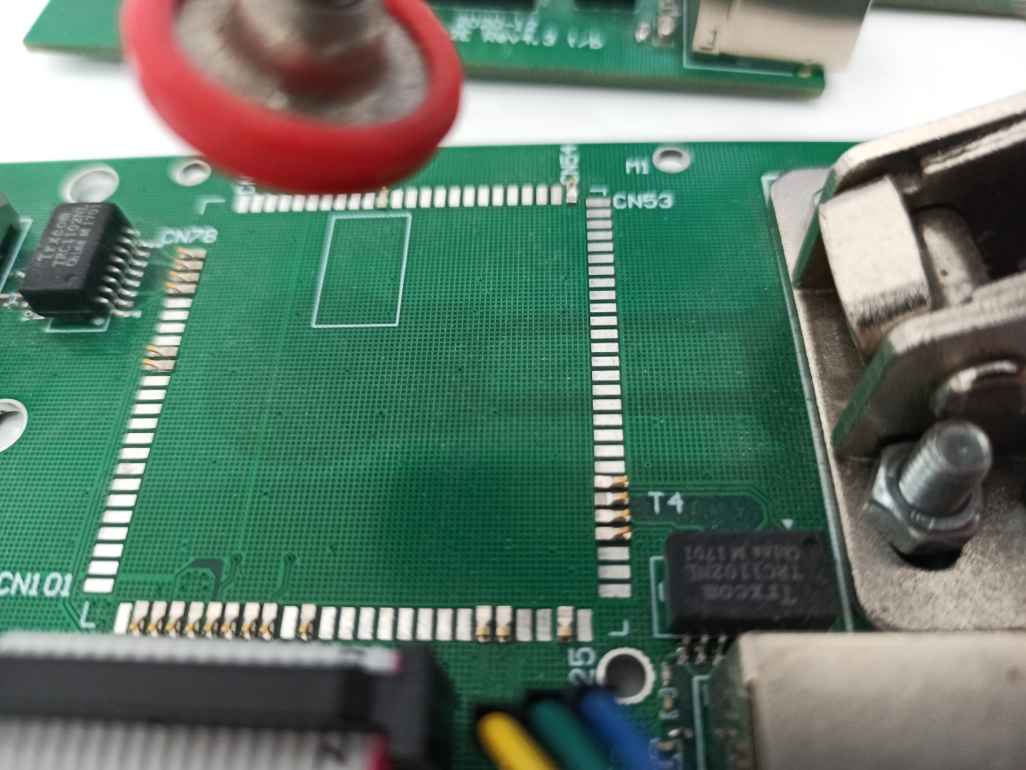
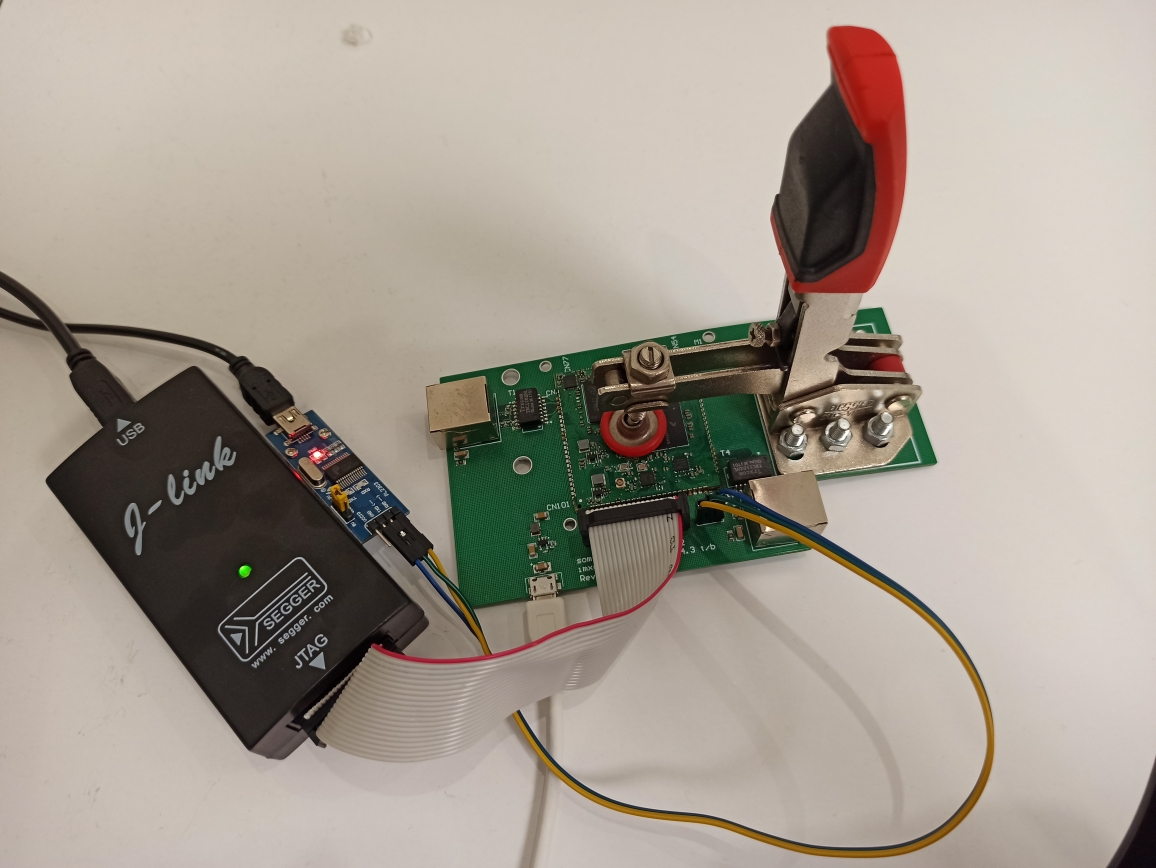
Hardware is trivial: spring connectors to place SoM. Fixation performs vertical toggle clamp. UART, JTAG and Ethernet routed to connect external USB-UART adapter, JTAG debugger and get access to local network.
When designing, there were some doubts about the durability of the testbench (especially regarding spring contacts) and positioning accuracy. But they were in vain. The stand survived at least several hundred tested modules.
Firmware flashing and burning of fuse bits
Firmware flashing and fuse-bits burning sequence:
- Install SoM-module to testbench and fix it
- connect USB-UART adapter, JTAG-interface, Ethernet cable and then power up testbench
- run openocd server:
11. write factory image to flash IC (COM-port console):
=> fuse prog -y 0 6 0x00000010
Automate it.
Steps from 3 to 13 can be easily automated. Here how it looks in Python:
# 1. Init OpenOCD server
device_state = Queue()
p_openocd = Process(target=run_openocd_server, args=(device_state,))
p_openocd.start()
check_state(device_state, STATE_JTAG_DEVICE_DETECTED)
# 2. Init. Connect to OpenOCD server via Telnet
telnet_socket_write_queue = Queue()
p_telnet = Process(target=run_telnet_client, args=(telnet_socket_write_queue,))
p_telnet.start()
check_state(device_state, STATE_TELNET_CLIENT_CONNECTED)
# 3. Init. Open COM port.
device_state_com = Queue()
com_port_write_queue = Queue()
p_com_port = Process(target=run_com_port_handler, args=(device_state_com,com_port_write_queue,CFG_COM_PORT,))
p_com_port.start()
# 4. Reset CPU
telnet_socket_write_queue.put((TELNET_CMD_RESTART_CPU + “\r\n”).encode())
check_state(device_state, STATE_CPU_RESET_COMPLETED)
# 5. Load u-boot image
telnet_socket_write_queue.put((TELNET_CMD_LOAD_U_BOOT_IMAGE + “\r\n”).encode())
check_state(device_state, STATE_IMAGE_LOADED, 30)
# 6. Load kernel image
telnet_socket_write_queue.put((TELNET_CMD_LOAD_KERNEL_IMAGE + “\r\n”).encode())
check_state(device_state, STATE_IMAGE_LOADED, 600)
# 7. Start U-boot execution
telnet_socket_write_queue.put((TELNET_CMD_START_U_BOOT + “\r\n”).encode())
check_state(device_state_com, STATE_U_BOOT_CONSOLE_ACCESSED)
# 8. Check flash IC available
com_port_write_queue.put(COM_CMD_CHECK_FLASH + “\r”)
check_state(device_state_com, STATE_FLASH_IC_DETECTED)
# 9. Flash firmware to IC
com_port_write_queue.put(COM_CMD_WRITE_FIRMWARE_TO_FLASH + “\r”)
check_state(device_state_com, STATE_FIRMWARE_FLASHED_TO_IC, 300)
# 10. Burn fuse bit (ECSPI3 programming 0x450 = 0x0a000030)
com_port_write_queue.put(COM_CMD_BURN_FUSE_BITS_1 + “\r”)
check_state(device_state_com, STATE_FUSE_BITS_BURNED)
# 11. Burn fuse bit (BT_FUSE_SEL programming 0x460 = 0x00000010)
com_port_write_queue.put(COM_CMD_BURN_FUSE_BITS_2 + “\r”)
check_state(device_state_com, STATE_FUSE_BITS_BURNED)
# 12. Reset device
com_port_write_queue.put(COM_CMD_RESET_DEVICE + “\r”)
TO-DO
replace step 6 (takes too much time) with factory image downloading using TFTP-server using u-boot tftp utility.